Wednesday, April 9, 2008

Input Output (LED 2)

More LED Blink

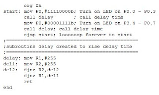
Congratulation, you have succeded with make a LED blink. Now lets improve your skill by making more LED blink ( 8 LED ). In this lesson, we will make four LED blink change reversed.

Step 1st
Build the circuit as shown in figure 1. As you seen on figure 2. P0.0 trough P0.7 is connected to LED's katode each. Remember, that all we want to do with this lesson is make four LED blink change reversed.

Figure 2. Diagram Skematik LED Blink

Step 2nd

In this step, you must tipe the assembly program to make four LED blink, we assume that you have already known the editor, we used MIDE-51 to edit the program.

Step 3rd
Safe your assembly program above, and name it with LED2.asm (for example) Compile the program that you have been save by using MIDE-51, see the software instruction.


Step 4th
Download your hex file ( LED2.hex ) into the microcontroller by using Microcontroller ATMEL ISP software, see the instruction.After download this hex file you'll see the action of the LED ( of course if your cable connection and your program are corrected ).

Thursday, April 3, 2008

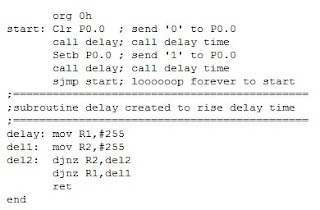
Input Output (LED 1)

L E D (Making a LED Blink)

The first step is to build a simple circuit. At this point you should be familiar with the parts used. (1 resistors, and 1 LED). This design is intended for use with an Atmel 89s51 but also posible for others family 8051. Most microcontrollers can handle the current required to turn an LED on and off but. In this lesson we're going to make a LED Blink continously.

Step 1st
Build the circuit as shown in figure 1. As you seen on figure 1 P0.0 is connected to LED's katode. Remember, that all we want to do with this lesson is make a LED blink.


Figure 1 Diagram Skematik LED Blink


Step 2nd
In this step, you must tipe the assembly program to make the LED blink, we assume that you have already known the editor, we used MIDE-51 to edit the program.


Step 3rd
Safe your assembly program above, and name it with LED1.asm (for example) Compile the program that you have been save by using MIDE-51, see the software instruction.


Step 4th
Download your hex file ( LED1.hex ) into the microcontroller by using Microcontroller ATMEL ISP software, see the instruction.After download this hex file you'll see the action of the LED ( of course if your cable connection and your program are corrected ).

Wednesday, April 2, 2008

Instruction Set

Arithmetic Instructions
The menu of arithmetic instructions is listed in Table 4.1 The table indicates the addressing modes that can be used with each instruction to access the operand.
For example, the ADD A, instruction can be written as:

ADD a, 7FH (direct addressing)
ADD A, @R0 (indirect addressing)
ADD a, R7 (register addressing)
ADD A, #127 (immediate constant)

The MUL AB instruction multiplies the Accumulator by the data in the B register and puts the 16-bit product into the concatenated B and Accumulator registers.
The DIV AB instruction divides the Accumulator by the data in the B register and leaves the 8-bit quotient in the Accumulator, and the 8-bit remainder in the B register.
Table 4.1. MCS-51 Arithmetic Instruction

Logical Instructions
Table 4.2 shows the list of 80C51 logical instructions. The instructions that perform Boolean operations (AND, OR, Exclusive OR, NOT) on bytes perform the operation on a bit-by-bit basis. That is, if the Accumulator contains 00110101B and byte contains 01010011B, then:
Table 4.2. MCS-51 Logical Instructions

Data Transfer
Internal RAM
Table 4.3 shows the menu of instructions that are available for moving data around within the internal memory spaces, and the addressing modes that can be used with each one. With a 12MHz clock, all of these instructions execute in either 1 or 2ms. The MOV , instruction allows data to be transferred between any two internal RAM or SFR locations without going through the Accumulator. Remember, the Upper 128 bytes of data RAM can be accessed only by indirect addressing, and SFR space only by direct addressing.The Data Transfer instructions include a 16-bit MOV that can be used to initialize the Data Pointer (DPTR) for look-up tables in Program Memory, or for 16-bit external Data Memory accesses.

Table 4.3. MCS-51 Data Transfer Instruction

Example:
a.
Org 0h
Start:Mov A,#1 ; put 1 into the accumulator
ADD A,#2 ; add the constant 2 to Accumulator (1+2)
Mov 78h,#3 ; put 3 into internal RAM 78h
ADD A, 78h ; add Acc and RAM 78h content
Mov R0, #79h; put 79 into R0
Mov @R0, #4 ; put 4 into RAM 79h
ADD A,@R0 ; add Acc and RAM 79h content
Mov R5, #5 ; put 5 into R5
ADD A,R5 ; add Acc and R5
end

b.
Org 0h
Start:Mov 78h,#34h ; [ 78h ] = 34h
Mov 79h,#12h ; [ 79h ] =12h
Mov 7Ah,#0EFh; [ 7Ah ] = EFh
Mov 7Bh,#12h ; [ 7Bh ] = 12h
Mov A,78h ; A = [ 78h ]
Add A,7Ah ; A = A + [ 78h ]
Mov 78h,A ; [ 78h ] = A
Mov A,79h ; A = [ 79h ]
ADDC A,7Bh ; A = A + [ 7Bh ] + C
Mov 79h,A ; [ 79h ] = A
end

Addressing

The addressing modes in the 80C51 instruction set are as follows:
An "addressing mode" refers to how you are addressing a given memory location. In summary, the addressing modes are as follows, with an example of each:

Immediate Addressing MOV A,#20h
Direct Addressing MOV A,30h
Indirect Addressing MOV A,@R0
External Direct MOVX A,@DPTR
Code Indirect MOVC A,@A+DPTR

Immediate Addressing
Immediate addressing is so-named because the value to be stored in memory immediately follows the operation code in memory. That is to say, the instruction itself dictates what value will be stored in memory.
For example, the instruction:

a.
;===========================================
;This instruction uses Immediate Addressing because the
;Accumulator will be loaded with the value that immediately
;follows in this case 20 (hexidecimal). ;===========================================
Org 0h
start:MOV A,#20h; put constant 20 into Acc
end

b.
Org 0h
Start:MOV A, #0h;
MOV A,#11h;
MOV B,#27h;
end

c.
Org 0h
Start:MOV 70h,#0h; put constant 0 into RAM 70h
MOV 71h,#1h;
MOV 72h,#2h;
end

d.
Org 0h
Start:MOV DPTR,#1234h; put constant 1234 into DPTR
end

e.
Org 0h
Start:MOV PSW,#0; Select register bank 0
MOV R0,#0; put 0 into register 0
MOV R1,#1; put 1 into register 1
MOV R2,#2; put 2 into register 2
MOV R3,#3; put 3 into register 3
MOV R4,#4; put 4 into register 4
MOV R5,#5; put 5 into register 5
MOV R6,#6; put 6 into register 6
MOV R7,#7; put 7 into register 7
end

f.
Org 0h
Start:MOV PSW,#8; Select register bank 1
MOV R0,#0; put 0 into register 0
MOV R1,#1; put 1 into register 1
MOV R2,#2; put 2 into register 2
MOV R3,#3; put 3 into register 3
MOV R4,#4; put 4 into register 4
MOV R5,#5; put 5 into register 5
MOV R6,#6; put 6 into register 6
MOV R7,#7; put 7 into register 7
end

Immediate addressing is very fast since the value to be loaded is included in the instruction. However, since the value to be loaded is fixed at compile-time it is not very flexible.

Direct Addressing
Direct addressing is so-named because the value to be stored in memory is obtained by directly retrieving it from another memory location. For example:

a.
;============================================
;This This instruction will read the data out of Internal
;RAM address 30 (hexidecimal) and store it in the
;Accumulator.
;============================================
; org 0h
Start:MOV A,30h;
end

b.
Org 0h
Start:Mov 70h,#1; put constant 1 into RAM 70h
Mov A, 70h; copy RAM 70 content into Acc
Mov A,#0 ;put constant 0 into Acc
Mov 90h,A ;copy Acc content into RAM 90h
end

c.
Inbyte equ 70h
Port1 equ 90h
Org 0h
Start: Mov Inbyte,#3;put constant 3 into RAM 70h
Mov A,Inbyte ;copy RAM 70h content into Acc
Mov A,#0 ;Clear accumulator
Mov Port1,A ;copy Acc content into RAM 90h
end

d.
Org 0h
Mov DPTR,#Character
Start:Mov A, #0
Inc DPTR
Movc A, @A+DPTR
Mov R0,A
Sjmp Start
Character:
DB 0,1,2,3,4,5,6,7,8,9

Direct addressing is generally fast since, although the value to be loaded isn’t included in the instruction, it is quickly accessable since it is stored in the 8051’s Internal RAM. It is also much more flexible than Immediate Addressing since the value to be loaded is whatever is found at the given address--which may be variable. Also, it is important to note that when using direct addressing any instruction which refers to an address between 00h and 7Fh is referring to Internal Memory. Any instruction which refers to an address between 80h and FFh is referring to the SFR control registers that control the 8051 microcontroller itself. The obvious question that may arise is, "If direct addressing an address from 80h through FFh refers to SFRs, how can I access the upper 128 bytes of Internal RAM that are available on the 8052?" The answer is: You can’t access them using direct addressing. As stated, if you directly refer to an address of 80h through FFh you will be referring to an SFR. However, you may access the 8052’s upper 128 bytes of RAM by using the next addressing mode, "indirect addressing."

Indirect Addressing
Indirect addressing is a very powerful addressing mode which in many cases provides an exceptional level of flexibility. Indirect addressing is also the only way to access the extra 128 bytes of Internal RAM found on an 8052.
Indirect addressing appears as follows:
MOV A,@R0
This instruction causes the 8051 to analyze the value of the R0 register. The 8051 will then load the accumulator with the value from Internal RAM which is found at the address indicated by R0. For example, let’s say R0 holds the value 40h and Internal RAM address 40h holds the value 67h. When the above instruction is executed the 8051 will check the value of R0. Since R0 holds 40h the 8051 will get the value out of Internal RAM address 40h (which holds 67h) and store it in the Accumulator. Thus, the Accumulator ends up holding 67h. Indirect addressing always refers to Internal RAM; it never refers to an SFR. Thus, in a prior example we mentioned that SFR 99h can be used to write a value to the serial port. Thus one may think that the following would be a valid solution to write the value ‘1’ to the serial port:
MOV R0,#99h ;
MOV @R0,#01h;
This is not valid. Since indirect addressing always refers to Internal RAM these two instructions would write the value 01h to Internal RAM address 99h on an 8052. On an 8051 these two instructions would produce an undefined result since the 8051 only has 128 bytes of Internal RAM.
a.
Org 0h
Start:Mov PSW, #0 ; choose register bank 0
Mov R0, #78h; put constant 78h into R0
Mov @R0, #1 ; put contanta 1 into 78h
end
b.
Org 0h
Start:Mov PSW,#0; pilih register bank 1
Mov R0,90h; copy RAM 90h content into R0
Mov @R0,#1; put constant 1 into 90h
end

External Direct
External Memory is accessed using a suite of instructions which use what I call "External Direct" addressing. I call it this because it appears to be direct addressing, but it is used to access external memory rather than internal memory.There are only two commands that use External Direct addressing mode:
MOVX A,@DPTR
MOVX @DPTR,A
As you can see, both commands utilize DPTR. In these instructions, DPTR must first be loaded with the address of external memory that you wish to read or write. Once DPTR holds the correct external memory address, the first command will move the contents of that external memory address into the Accumulator. The second command will do the opposite: it will allow you to write the value of the Accumulator to the external memory address pointed to by DPTR.

External Indirect
External memory can also be accessed using a form of indirect addressing which I call External Indirect addressing. This form of addressing is usually only used in relatively small projects that have a very small amount of external RAM. An example of this addressing mode is:
MOVX @R0,A
Once again, the value of R0 is first read and the value of the Accumulator is written to that address in External RAM. Since the value of @R0 can only be 00h through FFh the project would effectively be limited to 256 bytes of External RAM. There are relatively simple hardware/software tricks that can be implemented to access more than 256 bytes of memory using External Indirect addressing; however, it is usually easier to use External Direct addressing if your project has more than 256 bytes of External RAM.
Tuesday, April 1, 2008

Special Function Register

A Map of the on-chip memory area called the Special Function Register (SFR) space is shown in Figure 2.1. Note that in the SFRs not all of the addresses are occupied. Unoccupied addresses are not implemented on the chip. Read accesses to these addresses will in general return random data, and write accesses will have no effect. User software should not write 1s to these unimplemented locations, since they may be used in other 80C51 Family derivative products to invoke new features. The functions of the SFRs are described in the text that follows.


Figure 2.1. MCS-51 SFR Memory Map


Accumulator
ACC is the Accumulator register. The mnemonics for Accumulator-Specific instructions, however, refer to the Accumulator simply as A.
B Register
The B register is used during multiply and divide operations. For other instructions it can be treated as another scratch pad register.

Program Status Word
The PSW register contains program status information as detailed in Tabel 2.1

Stack Pointer
The Stack Pointer register is 8 bits wide. It is incremented before data is stored during PUSH and CALL executions. While the stack may reside anywhere in on-chip RAM, the Stack Pointer is initialized to 07H after a reset. This causes the stack to begin at locations 08H.

Data Pointer
The Data Pointer (DPTR) consists of a high byte (DPH) and a low byte (DPL). Its intended function is to hold a 16-bit address. It may be manipulated as a 16-bit register or as two independent 8-bit registers.

Ports 0 to 3
P0, P1, P2, and P3 are the SFR latches of Ports 0, 1, 2, and 3, respectively. Writing a one to a bit of a port SFR (P0, P1, P2, or P3) causes the corresponding port output pin to switch high. Writing a zero causes the port output pin to switch low. When used as an input, the external state of a port pin will be held in the port SFR (i.e., if the external state of a pin is low, the corresponding port SFR bit will contain a 0; if it is high, the bit will contain a 1).

Serial Data Buffer
The Serial Buffer is actually two separate registers, a transmit buffer and a receive buffer. When data is moved to SBUF, it goes to the transmit buffer and is held for serial transmission. (Moving a byte to SBUF is what initiates the transmission.) When data is moved from SBUF, it comes from the receive buffer.

Timer Registers
Register pairs (TH0, TL0), and (TH1, TL1) are the 16-bit Counting registers for Timer/Counters 0 and 1, respectively.

Control Register
Special Function Registers IP, IE, TMOD, TCON, SCON, and PCON contain control and status bits for the interrupt system, the Timer/Counters, and the serial port. They are described in later sections.


Table 2.1 Program Status Word


Program Status Word
The Program Status Word (PSW) contains several status bits that reflect the current state of the CPU. The PSW, shown in Figure 10, resides in the SFR space. It contains the Carry bit, the Auxiliary Carry (for BCD operations), the two register bank select bits, the Overflow flag, a Parity bit, and two user-definable status flags. The Carry bit, other than serving the function of a Carry bit in arithmetic operations, also serves as the “Accumulator” for a number of Boolean operations. The bits RS0 and RS1 are used to select one of the four register banks shown in Figure 1.7. A number of instructions refer to these RAM locations as R0 through R7. The selection of which of the four is being referred to is made on the basis of the RS0 and RS1 at execution time.

The Parity bit reflects the number of 1s in the Accumulator: P = 1 if the Accumulator contains an odd number of 1s, and P = 0 if the Accumulator contains an even number of 1s. Thus the number of 1s in the Accumulator plus P is always even. Two bits in the PSW are uncommitted and may be used as general purpose status flags.

Architecture of MCS-51 Microcontroller

Memory Organization.
All 80C51 devices have separate address spaces for program and data memory, as shown in Figures 1.1 and 1.2. The logical separation of program and data memory allows the data memory to be accessed by 8-bit addresses, which can be quickly stored and manipulated by an 8-bit CPU. Nevertheless, 16-bit data memory addresses can also be generated through the DPTR register. Program memory (ROM, EPROM) can only be read, not written to. There can be up to 64k bytes of program memory. In the 89s51, the lowest 4k bytes of program are on-chip. In the ROMless versions, all program memory is external. The read strobe for external program memory is the PSEN (program store enable).

Figure 1.1 89s51 Block Diagram

Data Memory (RAM) occupies a separate address space from Program Memory. In the 80C51, the lowest 128 bytes of data memory are on-chip. Up to 64k bytes of external RAM can be addressed in the external Data Memory space. In the ROMless version, the lowest 128 bytes are on-chip. The CPU generates read and write signals, RD and WR, as needed during external DataMemory accesses. External Program Memory and external Data Memory may be combined if desired by applying the RD and PSEN signals to the inputs of an AND gate and using the output of the gate as the read strobe to the external Program/Data memory.

Program Memory
Figure 1.4 shows a map of the lower part of the Program Memory. After reset, the CPU begins execution from location 0000H. As shown in Figure 1.4, each interrupt is assigned a fixed location in Program Memory. The interrupt causes the CPU to jump to that location, where it commences execution of the service routine. External Interrupt 0, for example, is assigned to location 0003H. If External Interrupt 0 is going to be used, its service routine must begin at location 0003H. If the interrupt is not going to be used, its service location is available as general purpose Program Memory.


Figure 1.2. Memory Program Structure


Figure 1.3. Interrupt Location


Data Memory
The right half of Figure 1.4 shows the internal and external Data Memory spaces available to the 80C51 user.The CPU generates RD and WR signals as needed during external RAM accesses. Internal Data Memory is mapped in Figure1.5. The memory space is shown divided into three blocks, which are generally referred to as the Lower 128, the Upper 128, and SFR space.

Figure 1.4. Memory Data Structure

Internal Data Memory addresses are always one byte wide, which implies an address space of only 256 bytes. However, the addressing modes for internal RAM can in fact accommodate 384 bytes, using a simple trick. Direct addresses higher than 7FH access one memory space, and indirect addresses higher than 7FH access a different memory space. Thus Figure 1.5. shows the Upper 128 and SFR space occupying the same block of addresses, 80H through FFH, although they are physically separate entities.


Figure 1.5. Internal Data Memory

The Lower 128 bytes of RAM are present in all 80C51 devices as mapped in Figure 1.6. The lowest 32 bytes are grouped into 4 banks of 8 registers. Program instructions call out these registers as R0 through R7. Two bits in the Program Status Word (PSW) select which register bank is in use. This allows more efficient use of code space, since register instructions are shorter than instructions that use direct addressing.

Figure 1.6. Lower 128 bytes of internal RAM

All of the bytes in the Lower 128 can be accessed by either direct or indirect addressing. The Upper 128 (Figure 1.7) can only be accessed by indirect addressing.

Figure 1.7.Upper 128 Bytes of Internal RAM